3D Machine Vision In The Electronics Industry
Machine vision technology has many advantages, and is advancing at a rapid pace.
The prospect of 3D machine vision technology holds the solution to many monitoring problems that depend on high precision results. By Hakan Thorngren, product manger, Vision Systems, Sick
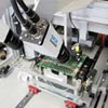
The electronics industry is one of the largest consumers of machine vision. The largest share of the cameras are being used for precise alignment in order to allow the equipment to handle the micro-metre precision required. Cameras for quality inspection are also integrated in ever increasing quantities.
The quality inspection ranges from checking the presence of selected parts on Printed Circuit Boards (PCBs) and product assemblies, to complete verifications of large PCBs with thousands of components. There are also cases where height information must be a parameter considered in the pass/fail decision. In those cases, 3D inspection is applied. Depending on the application, the height resolution required ranges from sub-micron to 100’s of microns.
Solder Paste Inspection
Solder paste inspection is a wide spread 3D application within electronics assembly. By adding an inspection station between the screen printer and the pick and place machine in the surface mount electronics assembly line, solder paste misprints can be captured before causing costly repairs.
The solder paste inspection must check that the right amount of paste is deposited on the PCB where it should be and nowhere else. The vision system must determine the x, y and z dimensions and calculate
the volume of the paste deposits — this calls for a 3D vision solution.
In addition, the vision system must also detect the presence of paste residues in the PCB areas that should not have any paste coverage. Since it is only about detecting the presence of paste contamination here, 2D vision is sufficient.
Two-dimensional colour imaging is beneficial since it gives better options to detect the paste residues on the PCB as the surface is green or other colour while the paste is grey.
An additional challenge is that a combination of high speed and high resolution is required. High resolution is needed to cope with paste deposits down to 125 x 125 x 100 µm in size, but vision systems also need to keep up with the line speed, and that calls for high speed.
Defective Components
Defective components are another source of errors in electronics assembly. When the pick and place machine mounts components on the PCB, it is vital that all the connection points of the component (terminals) are in contact with the solder paste. If this is not fulfilled the terminal will not get soldered, and therewith the electrical and mechanical connection is lost with a non-functioning product as a result.
To ensure that the component is safe to place, a so-called co-planarity inspection is made that verifies that all the terminals are within the same plane plus/minus a specified tolerance.
Co-planarity measurement systems can be applied either in the pick and place machines or as a final inspection step in the component manufacturing within the semiconductor backend industry.
In both areas the requirements of speed and resolution are comparable. The speed needs to be in the range of three components per second or better, and the resolution needs to be high in order to reach an accuracy below 10 µm/3-sigma which is recommended by industry standards.
The difference between the two areas is flexibility requirements. In the backend, the system operates in a batch manner, processing thousands of components of the same type while in pick and place the system must cope with one-offs — when one component is inspected, the next one coming a few hundred milliseconds later is likely to be of a completely different type. It calls for very careful system engineering and a very high system flexibility to cope with these variables.
Some electronic designs are also using high reliability connectors. Such connectors are often mounted using a press-fit assembly method. This is a solder free method of mounting through-hole components using a high-pressure mechanical press.
The component pins are shaped into springs and when pressed through the PCB, a gas-tight connection is formed with the plated PCB-hole. Even if the press-fit method has numerous advantages, it also comes with a unique set of challenges.
Before the press-fit, the component and PCB are pre-assembled in a very loose way, which is prone to errors. Proceeding and press-fitting an improperly made pre-assembly, will most probably result in a defective product. After the press-fit the contact between the PCB and pin is sufficient and reliable only if the designated part of the pin is in contact with the plated through-hole.
A visual inspection of the product before and after the press-fit is therefore highly beneficial. The key parameter to verify in both cases is the protrusion depth of the connection pins. Going for a 3D solution this is solvable by measuring the pin height on the backside of the PCB. The solution needs to be fast in order to cope with the line speed, it needs to provide the resolution required to image the thin pins, and it needs to be flexible and scalable to cope with the large variation of PCB-designs.
In Conclusion
Looking at the key features of the applications discussed, we conclude that the vision system has to be fast, have a high resolution and, on top of that, be flexible and scalable. The possibility to combine 3D imaging with 2D monochrome and colour imaging is also beneficial.
An ASIC design that contains photo-elements to capture the images, A/D-converters to digitise the image data as well as image processing functions that can create height profiles from the image data is suitable for such a task. The imager would also be addressable, allowing different areas of the imager to be used for different purposes. This opens up the possibility to acquire combinations of 3D, 2D monochrome and colour images at the same time.
By using several light sources in the setup; a line projecting laser for the 3D images by laser triangulation and a line light for the 2D images, the combination of 3D and 2D images can be acquired using the same camera. The scalability is further expanded through different resolution, speed and optical filtering options into a powerful and flexible concept that can be used together with standard components in terms of lenses, lighting and image processing libraries.
The use of one camera for all this has advantages; the solution can be made more compact; the cost is lower thanks to a reduced component count and finally less maintenance efforts are needed.
Lead/Bump Height Detection
Application Overview
When using modern assembly methods, like flip chip, CSP or fine pitch QFP, the electrical connection between the component and the substrate or PCB can only be ensured if all the bumps or leads are at reasonably the same height. To verify that this is the case a so-called co-planarity measurement is done.
This measurement is done by accurately measuring the height of each lead or bump, finding the three highest leads or bumps, and then measuring the deviation of each lead/bump to a plane touching the three highest bumps/leads.
True 3D Readouts
For the co-planarity the height of each lead or bump is the key factor to measure. Applying classical 2D inspection will only detect bumps and leads in the wrong place or with the wrong size. However with a 3D measurement system, both the 2D features and most importantly the height can be captured, solving the application to its full extent.
The Solution
The bumps are 3D scanned using the principle of laser triangulation. Every frame acquired generates one 3D-profile of the scene. Adding all the profiles acquired generates the full 3D view of the die and component. From an image analysis point of view, the 3D images can be processed in the same way as 2D images are processed. Comparing 2D and 3D image data, the contrast information in every pixel of a 2D image is replaced with a height value in a 3D image.
Calibration of measured data is given by the optics and triangulation geometry used, and by synchronising the profile acquisition with the scanning motion. Thanks to the high contrast between the laser line and the background, laser triangulation, as a principle, is very robust against stray light disturbances.